


November 24, 2023
The design teaching goal of PDS is to minimize the voltage ripple generated in response to the operating current requirements of the system power supply. All control circuits need to pass current, some circuits have a greater impact on market demand, and some circuits require us to provide a current at a faster rate.1oz vs 2oz With a sufficiently decoupled low-impedance power layer or ground condition and good PCB layering, the voltage ripple caused by the current information requirements of the circuit can be minimized. For example, if the company designs a switching current of 1A and the impedance of the PDS is 10mΩ, the maximum differential voltage ripple is 10mV.
First, you should design a PCB stack structure that supports a larger layer capacitor. For example, a six-layer stack may include a top signal layer, a first ground layer, a first power layer, a second power layer, a second ground layer,how to test a circuit board with a multimeter and a bottom signal layer. The first ground layer and the first power layer are close to each other in the stacked structure, and the spacing between the two layers is 2-3 ml to form a lamellar inherent capacitor. The main advantage of this capacitor is that it is free and only needs to be noted in the PCB manufacturing instructions. If you must split the power layer and have multiple VDD power rails in the same layer, use the largest possible power layer. Don't leave holes, and watch out for sensitive circuits. This will give the VDD layer a larger capacitance. If the design allows for additional layers (in this case from six to eight), two additional ground layers should be placed between the first and second power layers. When the core spacing is 2-3 mm, the inherent capacitance of the cascade structure will be doubled.
For an ideal PCB stack, decoupling capacitors should be used at the initial entry point of the power layer and around the DUT to ensure that the PDS impedance is low over the entire frequency range. Using multiple capacitors from 0.001μF to 100μF helps to cover this range. You don't need capacitors everywhere; Pairing a capacitor with a DUT breaks all manufacturing rules. If such drastic measures are needed, there are other problems in the circuit.
How to quickly distinguish the number of PCB boards on the motherboard
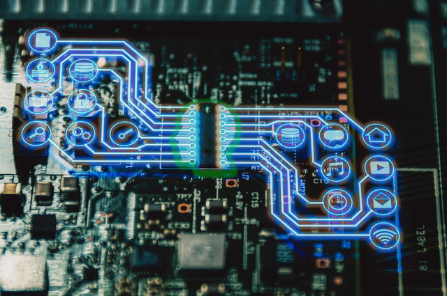
The importance of PCB design in electronic design
Two or three things you may not know about PCBS!
Posted by: sadabqbn at
03:55 AM
| Comments (23)
| Add Comment
Post contains 430 words, total size 3 kb.
34 queries taking 0.0604 seconds, 110 records returned.
Powered by Minx 1.1.6c-pink.

